Silicon
Board evidence, core cost, and fit
The physical ECP5 board has now exercised the loader, interpreter, monitor smoke path, and narrow PMP protections. The remaining sections give the supporting simulation and implementation-tool evidence: core cost, fit, and timing. Neither kind of evidence is presented as the other.
The source page has the interpreter itself and the transcripts showing it passes on this core. What those runs cost, and what silicon they need, is here.
What has run on the physical ECP5 board
The board is not a simulation result. USB/JTAG has repeatedly identified the selected LFE5UM5G-85F evaluation board, and volatile FPGA images have executed on its 12 MHz soft core. Configuration flash, expansion pins, and product outputs were not touched. On 27 September 2026 the confinement classes of the board jail-break series ran to completion against this image — canary-guarded interpreter probes, a user-mode PMP boundary sweep, the full CFS command space, wire-forgery shapes and a compute soak — and the boundary held under every one — series record.
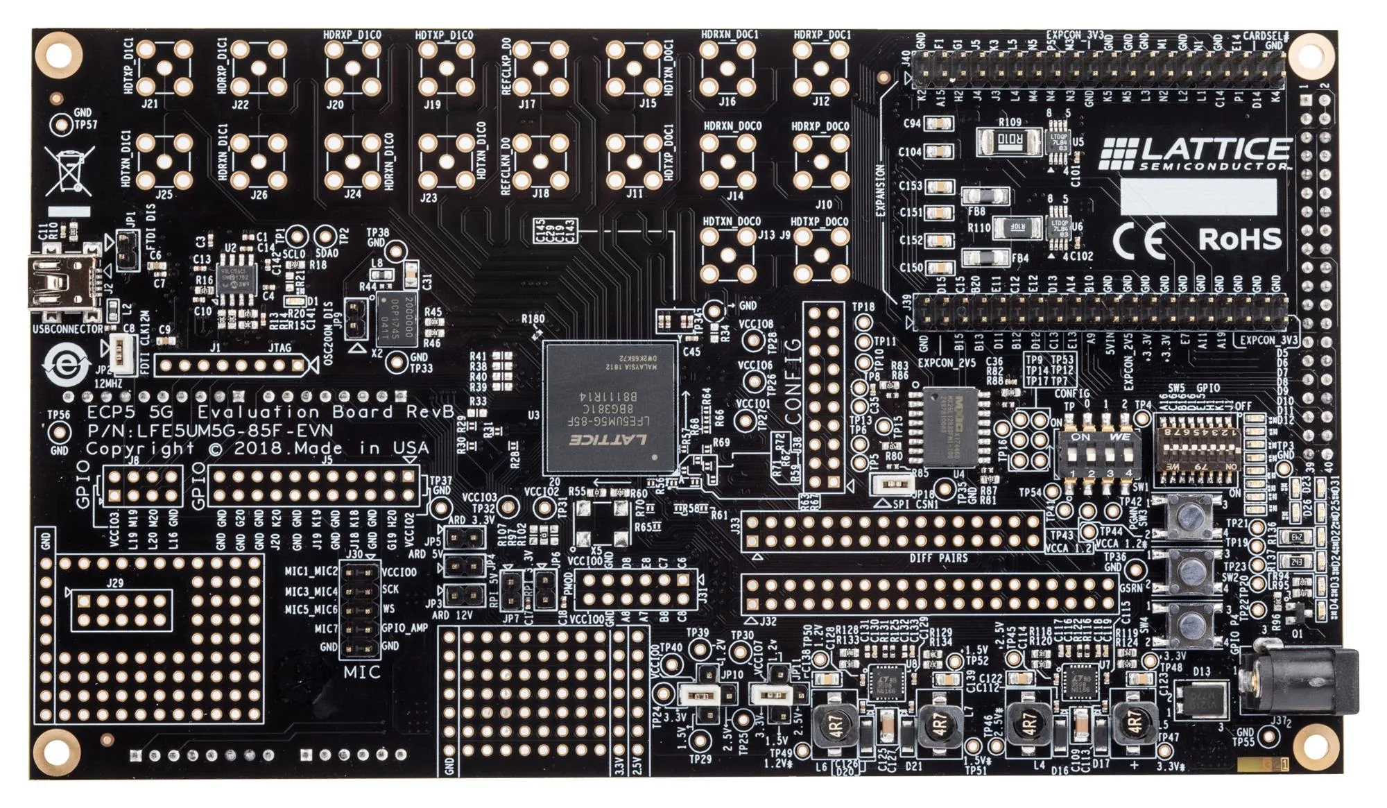

| Loader and interpreter path | 10,000 physical loader/VM iterations completed; the valid program produced its expected proposal and an invalid sequence was rejected |
|---|---|
| Monitor smoke | the loader/VM test image also exercised the monitor workload and ended on the observed four-middle-LED pass marker |
| Composite user-mode PMP sequence | an address-verified sentinel at RAM address 0x80000000 produced the expected store-access fault and load-access fault; a user-mode PMP-CSR write was also denied, then loader/VM/monitor smoke completed |
| Fabric-owned LED gate | a fabric safety policy mediates CFS requests to the LED gate; physical tests confirm that an inactive hardware arm blocks a direct request and that an armed permit expires into a lockout that rejects renewal. |
| Admission cost model on silicon | found, fixed and verified in public 27–28 September: the stub-measured capability entries under-charged a deployed propose 14.8× and the seal 57.9×; the table now carries measured callee bounds and every class runs within its charged credits on the board |
| PMP wall, fabric authority, wire protocol | 27 September, completing the jail-break series: a user-mode sweep of every region boundary faulted with its documented cause; the full 65,536-word CFS command space plus a rapid-refresh hammer produced zero permits and zero undocumented bits; nine wire-forgery shapes were each refused or silenced while the baseline frame was permitted; and the canary suite held 17/17 after a compute soak |
| Interpreter to physical arm | 26 September, PC-assisted rig: a program in the board's interpreter moved an SO-101 elbow 101 counts out and back, and a program one count past the envelope was refused before any actuator write; the trusted PC carried each approved goal to the servo |
Scope: volatile SRAM images on the ECP5 evaluation board, observed through LEDs and UART. The board drove no product outputs; in the arm row the trusted PC carried each approved goal to the servo.
Download the dated board
test record with board identity, source and bitstream hashes, and instrumentation limits →
Download the dated fabric-gate record →
Download the dated CFS fabric-gate record →
Download the dated physical-arm refusal record →
Download the dated fabric-policy disarm record →
Download the dated fabric-policy lockout record →
Download the dated VM-to-policy physical-disarm record →
Download the dated VM jail-break probe record →
Download the dated admission cost-rail record →
Download the dated cost-loop-closed record →
Download the dated interpreter-to-arm record →
Download the dated jail-break series J5–J8 record →
What different VM operations cost on this core
The interpreter now uses separate step fuel and timing credits. The first versioned timing table comes from a retained 38-row, no-cache NEORV32 RTL characterization. It is an engineering starting point, not hardware WCET.
| Fixed invocation overhead | 416 credits |
|---|---|
| ALU / multiply | 368 / 352 |
| Load byte / half / word | 336 / 368 / 432 |
| Store byte / half / word | 320 / 368 / 400 |
| Branch or jump | 448 |
| Capability 0 / 1 / 2 harness stubs | 480 / 464 / 480 |
| Exit / invalid path | 448 / 480 |
The harness used two jump baselines to separate fixed run overhead from marginal dispatch cost, then measured each class in a repeated mixed row. Credits are the observed class maxima plus 25%, rounded upward to 16 cycles. The complete binary, transcript, build log, hashes, tool versions, raw counts and limitations are retained in the dated simulator record.
Operational timing admission is not enabled. Capability rows used small harness stubs rather than deployed callees; exit and invalid paths were not isolated; and only one no cache configuration was characterized. Production use also requires an independent privileged deadline/watchdog. Step fuel still separately caps dispatches at 1,024 and proves termination even for loops.
Cache measurements. Three documents specified different configurations: the architecture page had no cache, the pilot plan enabled an i-cache, and the simulator defaulted to both caches. We ran all three. Each row below uses the same compiled image; only the generic changes.
| Configuration | Interpreter, cycles/insn | Monitor tick, worst | Both, share of a 2 ms tick |
|---|---|---|---|
| no cache ← published | 230.5 | 13,218 · 528.7 µs | 92.8% |
| i-cache only | 228.6 | 14,613 · 584.5 µs | 95.1% |
| i-cache + d-cache | 221.6 | 15,213 · 608.5 µs | 94.2% |
The two halves want opposite things. The interpreter is a tight dispatch loop and the caches help it; the monitor walks kinematic arrays with little reuse, so it pays a block fill on nearly every miss and gets few hits back. On this core that is not surprising — instruction and data memory are already on-chip block RAM, and a cache in front of memory that fast can cost more than it saves. The monitor's loss is the larger of the two, so the combined tick is cheapest with no cache at all, which is the configuration published above.
GHDL 7.0.0-dev (6.0.0.r176.g8bc05db0a) [Dunoon edition] · rustc 1.91.0-nightly (565a9ca63 2025-09-10)
· -gTRACE_LOG_EN=false -gDUAL_CORE_EN=false -gJTAG_TESTS_EN=false -gDMEM_SIZE=65536 -gIMEM_SIZE=131072
Eight runs, four parts, two memory configurations
| Target part | Block RAM | Logic (LUTs) | DSP | Speed | Fmax vs 25 MHz | Result |
|---|---|---|---|---|---|---|
| 128 KB instruction + 128 KB data | ||||||
| LFE5UM5G-85F | 130/ 208 | 5,063/ 83,640 | 4 / 156 | 8 | 96.2 MHz3.8× margin | Fits |
| LFE5U-85F | 130/ 208 | 5,063/ 83,640 | 4 / 156 | 6 | 62.0 MHz2.5× margin | Fits |
| LFE5U-45F | 130/ 108 | 5,063/ 43,848 | 4 / 72 | 6 | —never routed | Block RAM |
| LFE5U-25F | 130/ 56 | 5,063/ 24,288 | 4 / 28 | 6 | —never routed | Block RAM |
| 64 KB instruction + 64 KB data | ||||||
| LFE5U-85F | 66/ 208 | 4,912/ 83,640 | 4 / 156 | 6 | 76.5 MHz3.1× margin | Fits |
| LFE5U-45F | 66/ 108 | 4,912/ 43,848 | 4 / 72 | 6 | 74.4 MHz3.0× margin | Fits |
| LFE5U-25F | 66/ 56 | 4,912/ 24,288 | 4 / 28 | 6 | —never routed | Block RAM |
| LFE5U-12F | 66/ 56 | 4,912/ 24,288 | 4 / 28 | 6 | —never routed | Block RAM |
4 of the 8 runs place and route. The logic column never decides one of them: the design occupies between 6% and 23% of every part in the table, and it is never what fails. Block RAM is decided almost entirely by how much instruction and data memory the configuration asks for. The 128 + 128 KB split is inherited from a reference setup and has no workload-derived basis. The loadable image is about 3.2 KB against the 128 KB of instruction memory reserved for it.
The bar under each figure is drawn against that part's own ceiling, so a row that overflows is a row whose bar runs past the line.
Two rows carry identical utilisation and very different frequencies, and the speed column is most of the reason. The 5G part exists only in speed grade 8, and the tool refuses to build it at anything slower; the plain 85F defaults to grade 6, which is the grade the ULX3S carries. Forced to grade 8, the plain part increases from 61.7 to 82.2 MHz. The remaining gap comes from a difference between two device databases. Every row here is router seed 1, which is what makes the table and the sweep below comparable at all.
The same design, five router seeds
The pilot configuration on the eval-board part, placed and routed five times. All five pass; the worst clears the 25 MHz target by 3.6×. One pass would have been an anecdote. The router is seed-dependent by design, and a reported regression on the ice40 side of the same tool missed timing on 35 of 64 seeds in one build and 5 of 64 in another. We therefore report five seeds. That report also describes results that differ between runs at a fixed seed, for a cause that was never established, which is why the router build is pinned and named at the foot of this page.
And what it cost in fabric
The sweep above is a cycle result, and it decided the configuration. This is the same decision seen from the other tool: the design was first synthesised with the i-cache the pilot plan asked for, and then again without it once the cycle sweep had ruled it out. Same host, same toolchain, same five router seeds; one generic differs.
| Resource | i-cache | no cache ← published | Change |
|---|---|---|---|
| LUTs | 5,476 | 5,063 | -7.5% |
| Flip-flops | 1,879 | 1,770 | -5.8% |
| Block RAM | 130 | 130 | no change |
| Distributed RAM | 80 | 42 | -47.5% |
| Fmax, best of five seeds | 108.1 MHz | 102.5 MHz | -5.1% |
| Fmax, median seed | 98.2 MHz | 96.2 MHz | -2.0% |
Removing the cache cut LUT use by about 7% and distributed RAM use by half. Block RAM did not change. This disproved our published explanation that the cache pushed the design two blocks beyond the memory map. Removing it also failed to improve the clock: the median seed was slightly slower, and the two distributions overlap. We found no measurable timing effect.
The control-tick result still decides the configuration. We include the timing result because the table alone could suggest that the cache helped.
Two other questions the run answered
The fast multiplier is inferred: 4 of 156 DSP blocks. This was the largest named hardware risk in the design. The multiply either maps onto dedicated silicon or falls back to logic, and the difference is four cycles against thirty-five on the operation the signature is built from. It inferred.
Memory protection costs about 1,533 LUTs and 22% of the clock. Memory protection carries much of the assurance argument, and this run prices it. Eight regions with both addressing modes take 1.9% of the part and still clear 25 MHz by 3.0×.
What stands behind the rows
The fit rows above are one of four kinds of evidence behind this design. The ledger names the kind behind each claim, from machine-checked proofs to runs on the physical board.
How this page is produced
Frequencies on this page are place-and-route results from the open toolchain named below. They are engineering evidence, not assessment credit.
The artefact behind this page is site/fit-evidence.json, and the page is
generated from it. The flow that produces the artefact is published as
endstop-fit/run.sh.
Yosys 0.68+40 (git sha1 0f2bcb94b-dirty, Release, Clang /usr/local/osxcross/target/bin/aarch64-apple-darwin25.5-clang++ 21.1.8) · "nextpnr-ecp5" -- Next Generation Place and Route (Version nextpnr-0.10-122-gc73affb3)
· oss-cad-suite 2026-08-08, darwin-arm64
github.com/stnolting/neorv32 @ 99ef4e9
· rv32imc + Zicntr + Zknh · CPU_FAST_MUL_EN, CPU_FAST_SHIFT_EN, no cache